In recent years, the physical limits of semiconductor manufacturing processes have gradually emerged, and Moore’s Law, which traditionally relies on geometric shrinkage, is facing major challenges. At the 2026 International Circuits and Systems Symposium (IEEE ISCAS) held in Shanghai recently, He Tingbo, director of Huawei and president of the semiconductor business unit, officially announced a new development principle in the semiconductor field called “Tao (τ) Law”. This new technology concept provides a new evolution route for the industry, and is expected to allow manufacturers to continue to break through the bottleneck of chip performance despite the lack of advanced extreme ultraviolet (EUV) lithography machines.
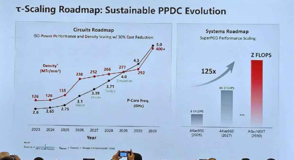
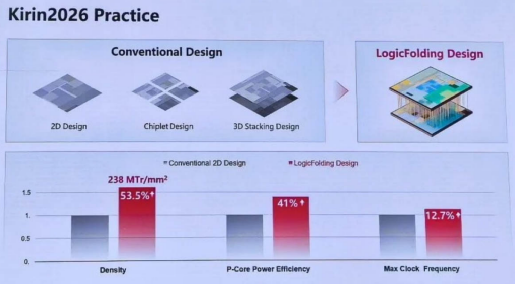
The core concept of “Tao’s Law” is to replace the traditional “geometric shrinkage” with “time shrinkage”. Simply put, this law aims to systematically reduce the time constant (τ) and continuously compress the signal propagation delay within the chip through innovative technical structures such as “logic folding”. This multi-level collaborative optimization system that runs through devices, circuits, chips and even system levels can effectively improve the overall transistor density and computing performance without relying solely on reducing the physical size of transistors. It provides a solution to the exponentially rising demands for artificial intelligence and high-end computing.
For the majority of smartphone users, this brand-new technology is by no means just talk on paper. Huawei officials revealed that in the past six years, they have successfully designed and mass-produced up to 381 types of chips based on this set of laws. The most eye-catching thing is that Huawei has announced that it will officially launch a new generation of Kirin mobile phone chips this fall. This new work will fully adopt logic folding technology, which is expected to significantly improve related performance and performance. This is undoubtedly a boost for Huawei’s upcoming new flagship phone. I believe many users are looking forward to its actual computing power and power consumption control performance in the future.
Looking forward to the future semiconductor technology blueprint, Huawei is confident in the development potential of “Tao’s Law”. The manufacturer predicts that by 2031, the transistor density of high-end chips designed based on this law will reach the same level as that of the equivalent 1.4nm process. He Tingbo emphasized at the meeting that future semiconductor development must be open and collaborative. Huawei hopes to communicate closely with scientists, engineers and industry partners around the world within the framework of the new laws. This technology release not only demonstrates Huawei’s deep strength in underlying chip research and development, but also means that the global semiconductor industry may usher in a major change away from reliance on traditional equipment.